The thermal expansion coefficient of the glass substrate is less than 10ppm/k, the breakdown voltage is above 6000V/m, and the surface flatness is extremely high, and its circuit board can be used for COG packaging of high-precision and low-power chips, such as Mini-LED chips, IC chips, microprocessor chips, etc.
This product uses micro-nano composite metal powder as the core of sintered copper paste or nickel paste, make glass-based circuit by additive manufacturing, which can replace single-sided aluminum substrate or double-sided BT board. The use of full dry process, on the surface of more than 2mm thick high-strength tempered glass ,rapidly print the sintered conductive lines and pads, for mounting a variety of low-power components, especially suitable for outdoor LED lights, indicator sign products. Baroy adopts the full additive process, making a precision double-sided circuit with a conduction hole on a 0.2∽0.7mm ultra-thin glass substrate, which is directly used to mount various low-power chips, especially suitable for the production of Mini-LED backlight boards.
Glass Substrate
• Lower material cost than aluminum substrate or BT material
• Thermal stability far superior to BT substrate, suitable for large-size high-precision SMT
• Surface flatness and roughness close to that of silicon wafers
• The thermal conductivity is comparable to that of ordinary aluminum substrates, which can efficiently dissipate heat over a large area
• Breakdown voltage above 6000V, reduce the cost of external transformer
Thick Metal Conductive Paste
• Base metal circuits, no risk of ion migration
• Electric conductivity 3.5μΩ·cm, close to the one of conventional PCB
• Peel strength 5N/mm, 6 times than that of conventional PCB
• 500°C high temperature fusion inorganic interface, thermal shock, environmental aging performance is good enough
Additive/Dry Manufacturing
• At least 3 steps to complete graphics circuit development, low process cost
• 100% utilization rate of conductive metal paste
• Line accuracy of 15μm, exceeding the PCB limits
• Dry process without water pollution
• Fully inorganic material, high voltage resistance; Anti-ultraviolet aging, anti-seawater corrosion
Application
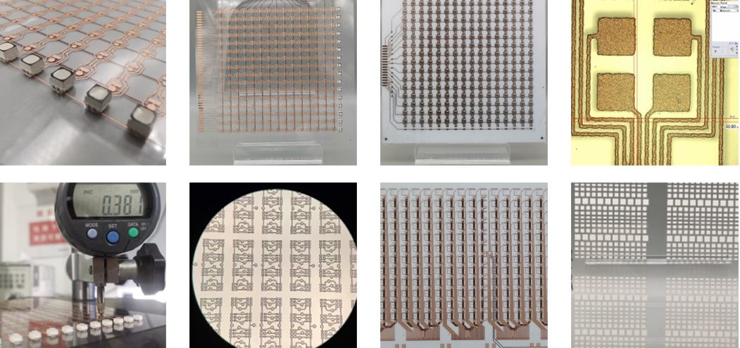
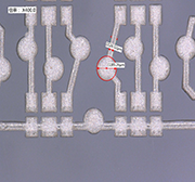
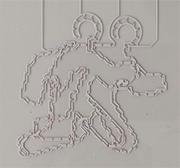

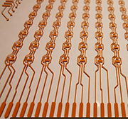
Specification:
Substrate Material |
| Ultra thin glass | Tempered Glass |
Coefficient of thermal expansion | <9 ppm/K | <10ppm/K |
Flexural strength | >120MPa | 600MPa |
Size | <250mmX350m | <250mmX350m |
Board Thickness | >0.2mm | >1.8mm |
Double size or not | √ | × |
Holes Diameter | >35μm | - |
Electric Conductive Material |
| Copper Circuits | Nickle/Silver Circuits |
Resistivity | 3.5μΩ·cm | 80μΩ·cm |
Line width/line spacing | Printing:>100μm Groove fill-in:>15μm | Printing:>150μm Groove fill-in:>35μm |
Line thickness | Printing:8∽35μm Groove fill-in:5∽300μm | Printing:15∽35μm Groove fill-in:10∽300μm |
Surface roughness | >0.3μm | >0.8μm |
Solder pad surface treatment | OSP、Immersion Silver | Sintering Silver |
Adhesion | >2N/mm | >5N/mm |