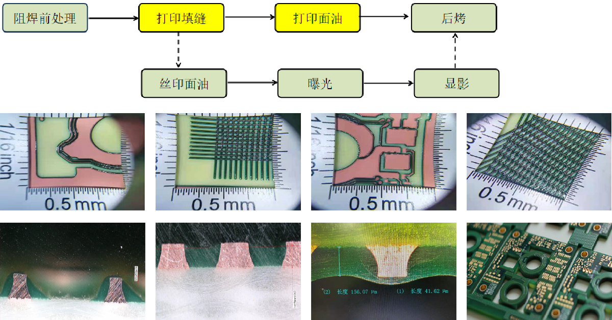
- Problem Description:For second power supply PCB and adapter PCB with large current-carrying and high voltage standing, when copper thickness > 5oz heavy copper boards, due to the relatively high copper surface of the line, the traditional dry film or wet film silk screen printing solder mask ink needs to be exposed and developed 2-3 times to achieve such heavy thickness of the specific solder mask, and the process is relatively long and no so cost effectiveness.
- Solution:For 5OZ or more heavy copper PCBs, the adoption of Baroy's 3D solder mask inkjet printing technology can make the production process shorter and high effectively , save more manpower and equipment investment, such solder mask inkjet printing technology with high exposure accuracy and meet IPC standard, on time delivery assurance as well.
Had been adopted by some PCBs manufacturers in mass production.
Above 5OZ thick copper plate inkjet resist production process:

Types | Normal Solder Mask | Inkjet Solder Mask | Inkjet void filling and surface printing by Solder Mask+ |
Process | Long Process 2-3 times repeat the solder mask exposure and development | Short Process 1 time solder mask development | Short Process 1 time inkjet printing+1 time exposure and development |
Capabiliy | Good high exposure precision | Average Inkjet Printing precision is second to exposure& Development processing | Good high exposure precision |
Visual | Acceptable | TBD | Acceptable |
Reliability | Meet The IPC Standard | Meet The IPC Standard | Meet The IPC Standard |